TNANO Article in focus: November 2016

From the November 2016 issue of IEEE Transactions on Nanotechnology

Continuous Fabrication of Multiscale Compound Eyes Arrays With Antireflection and Hydrophobic Properties

by Linfa Peng; Chengpeng Zhang; Hao Wu; Peiyun Yi; Xinmin Lai; Jun Ni
T-NANO, Vol. 15, Issue 6, pp. 971 – 976, November 2016.
 
nov2016
Images of the multi-scale compound eyes arrays: (a) low magnification image of multi-scale compound eyes arrays, (b) close-up image of the single microlens and its surroundings, (c) AFM image of the ordered array of tapered pillars.
Abstract: The multiscale hierarchical structures inspired by moth’s compound eyes offer multifunctional properties in optoelectronic devices. However, it is still a major challenge to fabricate these hierarchical structures on large-area substrates using a simple and cost-effective technique. The roll-to-roll ultraviolet nanoimprint lithography (R2R UV-NIL) technique provides a solution for the continuous fabrication of multiscale compound eyes arrays due to its high-speed, large-area, high-resolution, and high-throughput. In this paper, the R2R UV-NIL technique was used to fabricate the multiscale compound eyes arrays on the PET substrate. The mold used in the R2R UV-NIL process was acquired by anodic aluminum oxide process and then the multiscale compound eyes arrays were directly obtained via one-step R2R imprinting. The obtained multiscale compound eyes arrays exhibit excellent antireflective performance within the wavelength 400-800 nm. Besides, the compound eyes arrays also equip the surface of the microlens with excellent hydrophobic characteristics. These multifunctional properties enable the multiscale compound eyes arrays to retain their superior optical properties in real-time environmental conditions. This report can provide a beneficial direction for the continuous production and widespread applications of the multiscale compound eyes arrays.


TNANO Article in focus: October 2016

From the September 2016 issue of IEEE Transactions on Nanotechnology

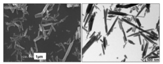
Halloysite Clay Nanotubes as Carriers for Curcumin: Characterization and Application

by Chiara Dionisi ; Nemany Hanafy ; Concetta Nobile ; Maria Luisa De Giorgi ; Ross Rinaldi ; Sergio Casciaro ; Yuri M. Lvov ; Stefano Leporatti
T-NANO, Vol. 15, Issue 5, pp. 720 – 724, September 2016.
 
Immagine
Abstract: Halloysite is a nanostructured clay mineral with hollow tubular structure, which has recently found an important role as delivery system for drugs or other active molecules. One of these is curcumin, main constituent in the rhizome of the plant Curcuma Longa, with a series of useful pharmacological activities, hindered by its poor bioavalaibility and solubility in water. In this study, Halloysite clay nanotubes (HNTs) were characterized in terms of both structure and biocompatibility and they were used for curcumin delivery to cancer cells. The performed 3-(4, 5-dimethythiazol-2-yl)-2, 5-diphenyl-tetrazolium bromide (MTT) assay showed that HNTs have a high biocompatibility, also when coated with polymers, while curcumin is highly toxic for cancer cells. The release kinetics of curcumin from HNTs was investigated by the dialysis bag method, showing a slow and constant release of the drug, which can be further controlled by adding layers of polyelectrolytes to the external surface of the tubes. Successful polymer coating was followed by Zeta potential. The Trypan Blue assay showed a cytotoxic effect of loaded HNTs, proportional to the concentration of tubes and the incubation time. Successful HNTs uptake by breast cancer cells was demonstrated by Confocal Laser Scanning Microscopy images. All results indicate that HNTs are a promising carriers for polyphenol delivery and release.


Special Section on VLSI and Nanotech. Design Trends for Computing Innovations

Joint Special Section on VLSI and Nanotechnology Design Trends for Computing Innovations

IEEE Transactions on Nanotechnology and IEEE Transactions on Emerging Topics in Computing seek original manuscripts for a Special Section tentatively scheduled to appear in the September 2017 issues.
The topics of interest for this special section include:

  • VLSI Design: Design of ASICs, microprocessors/micro-architectures, embedded processors, digital systems, NoC, interconnects, memories, and FPGAs.
  • VLSI Circuits: digital circuits, chaos/neural/fuzzy-logic circuits, high-speed/low-power circuits.
  • Low Power and Power Aware Design: Circuits, micro-architectural techniques, thermal estimation and optimization, power estimation methodologies, and CAD tools.
  • Computer-Aided Design (CAD): Hardware /software co-design, logic and behavioral synthesis, logic mapping, simulation and formal verification, layout (partitioning, placement, routing, floor planning, compaction), algorithms and complexity.
  • Testing, Reliability, Fault-Tolerance: Digital testing, design for testability and reliability, online testing techniques, static and dynamic defect- and fault-recoverability, and variation-aware design.
  • Emerging Technologies & Post-CMOS VLSI: Analysis, circuits and architectures, modeling, CAD tools and design methodologies for nanotechnologies, molecular electronics, quantum devices, biologically-inspired computing, spintronic technology, CNT, MTJ, NML, PCM, PMC, and sensor and sensor networks, etc.

Submitted articles must not have been previously published or currently submitted for journal publication elsewhere. An extended version of an article appearing in a conference proceedings (and in particular, GLSVLSI 2016) can be submitted provided that it has substantially new content w.r.t. to the original conference version. The conference paper must be cited in the main text and the cover letter must clearly describe the differences with the conference version and clearly identify the new contributions. As an author, you are responsible for understanding and adhering to the submission guidelines. Authors are invited to submit manuscripts focused on topics of computing directly to Transactions on Emerging Topics in Computing (TETC) at https://mc.manuscriptcentral.com/tetc-cs and papers focused on topics of nanoscale circuits and technology directly to Transactions on Nanotechnology (TNano) at https://mc.manuscriptcentral.com/tnano. Authors should be aware that papers can be published in TNano or TETC depending on the availability of space with the final allocation at the discretion of the Editor-in-Chief of the respective Transactions. Please address all correspondence regarding this Special Section to the Guest Editors (email: tpc.chairs@gmail.com).

Important Dates

  • Manuscript Submission: November 1, 2016.
  • First decision to authors: February 1, 2017.
  • Revision due (if necessary): April 1, 2017.
  • Final notification (acceptance/rejection): July 1, 2017.
  • Final manuscripts due: August 1, 2017.
  • Special section publication: September 2017.

Guest Editors

 
Laleh Behjat (University of Calgary)
Ayse Coskun (Boston University)
Jie Han (University of Alberta)
Martin Margala (University of Massachusetts Lowell)
The Call for Papers is available here


TNANO Article in focus: September 2016

From the September 2016 issue of IEEE Transactions on Nanotechnology

Methodology and Design of a Massively Parallel Memristive Stateful IMPLY Logic-Based Reconfigurable Architecture

by YYasunao Katayama; Toshiyuki Yamane; Daiju Nakano; Ryosho Nakane; Gouhei Tanaka
T-NANO, Vol. 15, Issue 5, pp. 762 – 769, September 2016.
 
Immagine
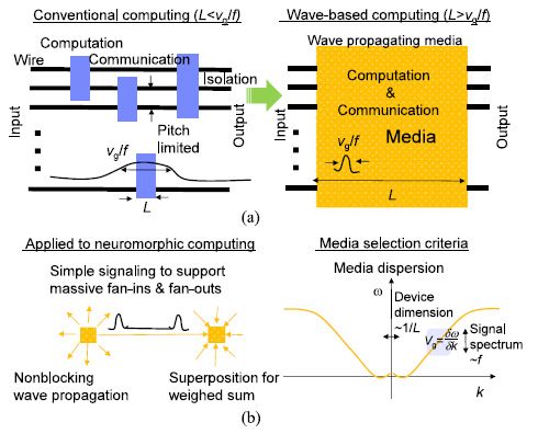
Abstract: We present a framework of wave-based neuromorphic computing aiming at brain-like capabilities and efficiencies with nanoscale device integration. We take advantage of the unique nature of elastic nondissipative wave dynamics in both computations and IO communications in between as a means to natively implement and execute neuromorphic computing functions such as weighted sum in a spatiotemporal manner. Lower bound analysis based on a memory model and wave group velocity scaling is provided for conceptual evaluations.
 

TNANO Article in focus: August 2016

From the July 2016 issue of IEEE Transactions on Nanotechnology

Methodology and Design of a Massively Parallel Memristive Stateful IMPLY Logic-Based Reconfigurable Architecture

by Kamela C. Rahman; Dan Hammerstrom; Yiwei Li; Hongyan Castagnaro; Marek A. Perkowski
T-NANO, Vol. 15, Issue 4, pp. 675 – 686, July 2016.
 
teaser0816
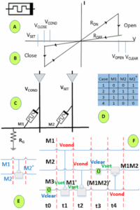
Abstract: Continued dimensional scaling of CMOS processes is approaching fundamental limits and, therefore, alternate new devices and microarchitectures are explored to address the growing need of area scaling and performance gain. New nanotechnologies, such as memristors, emerge. Memristors can be used to perform stateful logic with nanowire crossbars, which allows for implementation of very large binary networks. This paper involves the design of a memristor-based massively parallel datapath for various applications, specifically single instruction multiple data and parallel pipelines. The innovation of our approach is that the datapath design is based on space-time diagrams that use stateful IMPLY gates built from binary memristors. The paper also develops a new model and methodology to design massively parallel memristor-CMOS hybrid datapath architectures at a system level. This methodology is based on an innovative concept of two interacting subsystems: 1) a controller composed of a memristive RAM, MsRAM, to act as a pulse generator, along with a finite-state machine realized in CMOS, a CMOS counter, CMOS multiplexers, and CMOS decoders; 2) massively parallel pipelined datapath realized with a new variant of a CMOL-like nanowire crossbar array, memristive stateful CMOL with binary stateful memristor-based IMPLY gates. In contrast to previous memristor-based FPGA, our proposed memristive stateful logic field programmable gate array uses memristors for both memory and combinational logic implementation. With a regular structure of square abutting blocks of memristive nanowire crossbars and their short connections, our architecture is highly reconfigurable. We present the design of a pipelined Euclidean distance processor along with its various applications. Euclidean distance calculation is widely used by many neural network and similar algorithms.
 

Special Issue on the IEEE International Conference on Nanotechnology

Special Section/Issue on the IEEE International Conference on Nanotechnology

IEEE Transaction on Nanotechnology (TNANO) seeks original research manuscripts for a Special Section/Issue on the IEEE 2016 IEEE International Conference on Nanotechnology.

Background and Scope

 
Extensive research on nanotechnology materials and devices has unveiled many interesting and promising applications in electronics, photonics, biomedicine, and beyond. Encouraged by the success of the IEEE 16th International Conference on Nanotechnology (IEEE NANO 2016), IEEE Transactions on Nanotechnology (TNANO) will consider extended/revised versions of papers presented at IEEE NANO 2016. Submitted manuscripts will undergo a full peer review process.
Authors are requested to revise/expand the conference version to contain substantial new technical materials due to the restriction in duplicated publications and the competitive acceptance process.
Manuscripts for TNANO must be submitted on-line using the IEEE TNANO manuscript template and “Information for Authors”, via the IEEE Manuscript Central found at https://mc.manuscriptcentral.com/tnano. On submission to TNANO, authors should select the “Special Issue” manuscript type instead of “Regular Paper.” Manuscripts must focus on nanotechnology as reflected by technical contents and references.
Important Dates

  • Manuscript Submission: September 31, 2016
  • First decision to authors: November 31, 2016
  • Revision due (if necessary): December 30, 2016
  • Final notification (acceptance/rejection): February 15, 2017
  • Final manuscripts due: March 15, 2017
  • Special section publication: 2017

Guest Editors

 
Please address all other correspondence regarding this Special Issue to the Guest Editors:
Prof. Takahito Ono (Tohoku University, Japan)
E-mail: ono@nme.mech.tohoku.ac.jp
Prof. Ichiro Yamashita (Nara Institute of Science and Technology, Japan)
E-mail: ichiro@ms.naist.jp
Prof. Yming Li (National Chiao Tung University, Taiwan)
E-mail: ymli@faculty.nctu.edu.tw
Prof. Sreeram Vaddiraju (Texas A&M University, USA)
E-mail: sreeram.vaddiraju@tamu.edu
Prof. Chang-ki Baek (Pohang University of Science and Technology, Korea)
E-mail: baekck@postech.ac.kr
The Call for Papers is available here


Special Issue on the IEEE Nanotechnology Materials and Devices Conference

Special Section/Issue on the IEEE Nanotechnology Materials and Devices Conference

IEEE Transaction on Nanotechnology (TNANO) seeks original research manuscripts for a Special Section/Issue on the IEEE Nanotechnology Materials and Devices Conference.

Background and Scope

 
Extensive research on nanotechnology materials and devices has unveiled many interesting and promising applications in electronics, photonics, biomedicine, and beyond. Encouraged by the success of the IEEE Nanotechnology Materials and Devices Conference (IEEE NMDC), IEEE Transactions on Nanotechnology (TNANO) will consider extended/revised versions of papers presented at IEEE NMDC 2016. Submitted manuscripts will undergo a full peer review process.
Authors are requested to revise/expand the conference version to contain substantial new technical materials due to the restriction in duplicated publications and the competitive acceptance process.
Manuscripts for TNANO must be submitted on-line using the IEEE TNANO manuscript template and “Information for Authors”, via the IEEE Manuscript Central found at https://mc.manuscriptcentral.com/tnano. On submission to TNANO, authors should select the “Special Issue” manuscript type instead of “Regular Paper.” Manuscripts must focus on nanotechnology as reflected by technical contents and references.
Important Dates

  • Manuscript Submission: October 30, 2016
  • First decision to authors: December 30, 2016
  • Revision due (if necessary): January 30, 2017
  • Final notification (acceptance/rejection): March 15, 2017
  • Final manuscripts due: April 15, 2017
  • Special section publication: 2017

Guest Editors

 
Please address all other correspondence regarding this Special Issue to the Guest Editors:
Fuccio CRISTIANO
E-mail: cristiano.fuccio@laas.fr
Nicolas GHERARDI
E-mail: nicolas.gherardi@laplace.univ-tlse.fr
The Call for Papers is available here.


TNANO Article in focus: July 2016

From the July 2016 issue of IEEE Transactions on Nanotechnology

Effect of a Clock System on Bis-Ferrocene Molecular QCA

by Ruiyu Wang, Azzurra Pulimeno, Massimo Ruo Roch, Giovanna Turvani, Gianluca Piccinini, Mariagrazia Graziano
T-NANO, Vol. 15, Issue 4, pp. 574 – 582, July 2016.
 
teaser0716
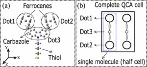
Abstract: Molecular quantum-dot cellular automata (mQCA) is found to be the most promising among all emerging technologies. It is expected to show remarkable operating frequencies (THz), high device densities, noncryogenic working temperature, and reduced power consumption. The computation relies on a new paradigm based on the interaction between nearby molecular QCA cells. This computation requires the aid of an external signal normally referred to as clock that enables/inhibits the molecular activity. The influence of clock on realistic molecules has never been deeply studied. In this paper, we performed a thorough analysis of the clock signal added to the molecular QCA cell based on an ad hoc synthesized bisferrocene molecule. Ab-initio simulations and further postprocessing of data have been used for characterizing the performance of bisferrocene molecule under the influence of a clock signal. Quantitative results on the molecule in terms of newly defined figures of merits, i.e., aggregated charge , equivalent voltage, and Vin-Vout transcharacteristic have been shown. Meanwhile, we demonstrate when and how much the presence of clock signal enhances or hinders the interactions between QCA molecules. These unprecedented data give a fundamental improvement to the knowledge on how information can be propagated through QCA devices. The results suggest directions to chemists, technologists, and engineers on how to proceed in the next steps for this promising technology.
 

Special Issue on Revolutionary 3-D Integration

Special Issue on Revolutionary 3-D Integration and Design for Next Generation Computing

IEEE Transaction on Nanotechnology (TNANO) seeks original research manuscripts for a Special Issue on Revolutionary 3-D Integration and Design for Next Generation Computing.

Background and Scope

 
As the scaling limitations of 2-D ICs are becoming more apparent, 3-D integration at nanoscale is emerging as an attractive alternative to continue IC scaling in the future. Driven by the benefits of less stringent lithographic dependence, multi-scale nature with reduced interconnections, higher packing density and smaller footprints, 3-D ICs promise to revolutionize the semiconductor and computing industries and enable unique new applications. Promising 3-D IC directions include nanoscale monolithic and fine-grained 3-D CMOS and beyond CMOS 3-D approaches, as well as heterogeneous technologies that are multi-scale in nature, with potentially orders of magnitude improved efficiencies. 3-D IC research often involves cross-disciplinary explorations at multiple scales, combining new technologies for manufacturing and devices with unique integration/design concepts. Targeting the broad device, circuit, and architecture, as well as nanotechnology research communities, this special issue seeks papers on innovative new concepts for such 3-D ICs. High-risk high-reward type of ideas, rethinking 3-D integration, and associated circuits and architectures, will be preferred to incremental research. Applications that are enabled by or show potential for significant benefits from 3-D integration are also welcome. Review papers presenting a broad overview of emerging 3-D technologies can be similarly submitted.
Topics of interest include but are not limited to the following:

  • 3-D IC integration and 3-D fabrics enabled by emerging nanotechnology.
  • 3-D memory and logic technologies.
  • 3-D routability.
  • 3-D circuit design exploration with CMOS and beyond CMOS directions.
  • 3-D circuit architectural exploration with CMOS and beyond CMOS directions.
  • Unconventional computing paradigms such as neuromorphic, probabilistic, sparse data and others, enabled by 3-D integration.
  • Gate and transistor-level monolithic 3-D CMOS directions.
  • Multi-scale, mixed-signal heterogeneous 3-D integrations.
  • 3-D design methodologies including thermal management.
  • New applications enabled by or significantly benefitting from 3-D integration.
  • Experimental proof-of- concept prototyping for small-scale demonstrations as well as scalable 3-D nanomanufacturing approaches. Directions may include multi-level epitaxial growth, wafer thinning, wafer bonding, and wafer alignment techniques, as well as others.

Submission Format

 
The submitted papers must be written in English and describe original research which is not published nor currently under review by other journals or conferences. Extended conference papers should contain at least 50% new material and will pass through the normal review process. Author guidelines for preparation of manuscript can be found at the IEEE Transactions on Nanotechnology website (https://site.ieee.org/tnano/author-info/).

Submission Guidelines

 
All manuscripts and any supplementary material should be submitted through the TNANO Manuscript Central (http://mc.manuscriptcentral.com/tnano). On submission, authors must select the “Special Issue” manuscript type instead of “Regular Paper”, and state in the cover letter that the paper is for the special issue on “Revolutionary 3-D Integration and Design for Next Generation Computing,’’ and select Csaba Moritz as the Preferred Editor.
Important Dates

  • Paper Submission: August 1, 2016 through December 1, 2016 (UPDATED)
  • Paper Submission: August 1, 2016 through January 14, 2017
  • Reviews Completed: March 1, 2017
  • Major Revisions Due (if Needed): April 1, 2017
  • Minor Revisions Due (if Needed): June 1, 2017
  • Notification of Final Acceptance: August 1, 2017
  • Final Manuscript Due: Sept 1, 2017
  • Tentative Publication Date: Late 2017

Guest Editors

 
Please address all other correspondence regarding this Special Issue to the Guest Editors using the following email-ID: 3dsi-tnano@googlegroups.com
Csaba Andras Moritz
Professor, Electrical and Computer Engineering
Director Nanofabrics Laboratory
University of Massachusetts Amherst, MA, USA
E-mail: andras@ecs.umass.edu
URL: http://www.ecs.umass.edu/ece/andras
Sung-Kyu Lim
Dan Fielder Professor
School of Electrical and Computer Engineering
Georgia Institute of Technology, Atlanta, GA 30332-0250, USA
E-mail: limsk@ece.gatech.edu
URL: http://users.ece.gatech.edu/limsk/
Kangwook Lee,
Professor, New Industry Creation Hatchery Center (NICHe)
Deputy Director, Global INTegration Initiative (GINTI)
Tohoku University, Japan
E-mail: kriss@bmi.niche.tohoku.ac.jp
Deepak Nayak
Distinguished MTS Global Foundries (3D Integration)
E-mail: deepak.nayak@globalfoundries.com
Mostafizur Rahman
Assistant Professor, Computer Science and Electrical Engineering
University of Missouri-Kansas City, MO, USA
E-mail: rahmanmo@umkc.edu
URL: http://sce2.umkc.edu/csee/rahmanmo/ (more…)

TNANO Article in focus: June 2016

From the May 2016 issue of IEEE Transactions on Nanotechnology

Smart Detector Cell: A Scalable All-Spin Circuit for Low Power Non-Boolean Pattern Recognition

by Hamidreza Aghasi ; Rouhollah Mousavi Iraei ; Azad Naeemi ; Ehsan Afshari
T-NANO, Vol. 15, Issue 3, pp. 356 – 366, May 2016.
 
teaserjune16
Abstract: We present a new circuit for non-Boolean recognition of binary images. Employing all-spin logic (ASL) devices, logic comparators and non-Boolean decision blocks for compact and efficient computation are designed. By manipulation of fan-in number in different stages of the circuit, the structure can be extended for larger training sets or larger images. Operating based on the main similarity idea, the system is capable of constructing a mean image and compare it with a separate input image within a short decision time. Taking advantage of the nonvolatility of ASL devices, the proposed circuit is capable of hybrid memory/logic operation. Compared with the existing CMOS pattern recognition circuits, this paper achieves a smaller footprint, lower power consumption, faster decision time, and a lower operational voltage.